- 您现在的位置:买卖IC网 > Sheet目录368 > W25X64VZEIG (Winbond Electronics)IC FLASH 64MBIT 75MHZ 8WSON
W25X16, W25X16A, W25X32, W25X64
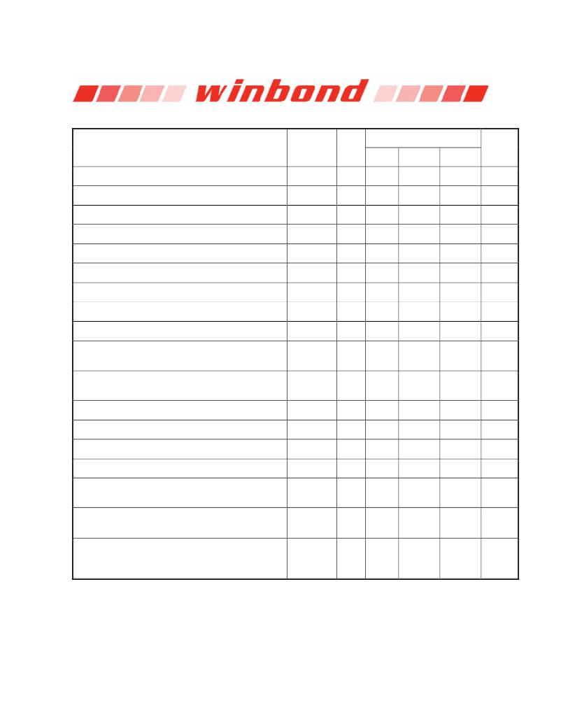
AC Electrical Characteristics (cont’d)
DESCRIPTION
/HOLD Active Setup Time relative to CLK
/HOLD Active Hold Time relative to CLK
/HOLD Not Active Setup Time relative to CLK
/HOLD Not Active Hold Time relative to CLK
SYMBOL
t HLCH
t CHHH
t HHCH
t CHHL
ALT
MIN
5
5
5
5
SPEC
TYP
MAX
UNIT
ns
ns
ns
ns
/HOLD to Output Low-Z
/HOLD to Output High-Z
Write Protect Setup Time Before /CS Low
Write Protect Hold Time After /CS High
/CS High to Power-down Mode
/CS High to Standby Mode without Electronic
t HHQX (2)
t HLQZ (2)
t WHSL (3)
t SHWL (3)
t DP (2)
t RES 1 (2)
t LZ
t HZ
20
100
7
12
3
3
ns
ns
ns
ns
μs
μs
Signature Read
/CS High to Standby Mode with Electronic
t RES 2 (2)
1.8
μs
Signature Read
Write Status Register Time
Byte Program Time (First Byte) (4)
Additional Byte Program Time (After First Byte) (4)
Page Program Time
Sector Erase Time (4KB) W25X16, W25X32
Sector Erase Time (4KB) W25X16A, W25X64
Block Erase Time (64KB) W25X16, W25X32
Block Erase Time (64KB) W25X16A, W25X64
Chip Erase Time W25X16
Chip Erase Time W25X16A
Chip Erase Time W25X32, W25X64
t W
t BP1
t BP2
t PP
t SE
t BE
t CE
10
30
6
1.6
150
120
0.8
0.32
25
10
40
15
50
12
3
300
200
2
1
40
20
80
ms
μs
μs
ms
ms
ms
s
s
s
s
s
Notes:
1.
2.
3.
4.
Clock high + Clock low must be less than or equal to 1/f C .
Value guaranteed by design and/or characterization, not 100% tested in production.
Only applicable as a constraint for a Write Status Register instruction when Sector Protect Bit is set to 1.
For multiple bytes after first byte within a page, t BPN = t BP1 + t BP2 * N (typical) and t BPN = t BP1 + t BP2 * N (max), where N
= number of bytes programmed.
- 38 -
发布紧急采购,3分钟左右您将得到回复。
相关PDF资料
W25X80AVDAIZ
IC FLASH 16MBIT 100MHZ 8DIP
W29GL032CB7A
IC FLASH 32MBIT 70NS 48TFBGA
W29GL064CB7S
IC FLASH 64MBIT 70NS 48TSOP
W29GL128CL9T
IC FLASH 128MBIT 90NS 56TSOP
W631GG6KB-15
IC DDR3 SDRAM 1GBIT 96WBGA
W9412G6IH-5
IC DDR-400 SDRAM 128MB 66TSSOPII
W9412G6JH-5I
IC DDR SDRAM 128MBIT 66TSOPII
W9425G6EH-5
IC DDR-400 SDRAM 256MB 66TSSOPII
相关代理商/技术参数
W25X64VZEIZ
制造商:WINBOND 制造商全称:Winbond 功能描述:16M-BIT, 32M-BIT, AND 64M-BIT SERIAL FLASH MEMORY WITH 4KB SECTORS AND DUAL OUTPUT SPI
W25X64VZPI
制造商:WINBOND 制造商全称:Winbond 功能描述:16M-BIT, 32M-BIT, AND 64M-BIT SERIAL FLASH MEMORY WITH 4KB SECTORS AND DUAL OUTPUT SPI
W25X64VZPIG
制造商:WINBOND 制造商全称:Winbond 功能描述:16M-BIT, 32M-BIT, AND 64M-BIT SERIAL FLASH MEMORY WITH 4KB SECTORS AND DUAL OUTPUT SPI
W25X64VZPIZ
制造商:WINBOND 制造商全称:Winbond 功能描述:16M-BIT, 32M-BIT, AND 64M-BIT SERIAL FLASH MEMORY WITH 4KB SECTORS AND DUAL OUTPUT SPI
W25X80
制造商:WINBOND 制造商全称:Winbond 功能描述:The W25X10 (1M-bit), W25X20 (2M-bit), W25X40 (4M-bit) and W25X80 (8M-bit) Serial Flash memories provide a storage solution for systems with limited space, pins and power.
W25X80A
制造商:WINBOND 制造商全称:Winbond 功能描述:1M-BIT, 2M-BIT, 4M-BIT AND 8M-BIT SERIAL FLASH MEMORY WITH 4KB SECTORS AND DUAL OUTPUT SPI
W25X80AL
制造商:WINBOND 制造商全称:Winbond 功能描述:1M-BIT, 2M-BIT, 4M-BIT AND 8M-BIT 2.5V SERIAL FLASH MEMORY WITH 4KB SECTORS AND DUAL OUTPUT SPI
W25X80ALDAIG
制造商:WINBOND 制造商全称:Winbond 功能描述:1M-BIT, 2M-BIT, 4M-BIT AND 8M-BIT 2.5V SERIAL FLASH MEMORY WITH 4KB SECTORS AND DUAL OUTPUT SPI
